
White House / October 09, 2021
New plan aims to accelerate research translation, advance equity
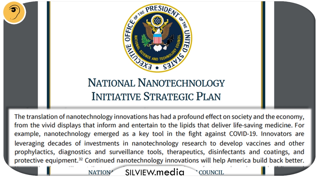
Today, on National Nanotechnology Day, the White House Office of Science and Technology Policy (OSTP) and the National Nanotechnology Coordination Office (NNCO) unveiled the 2021 National Nanotechnology Initiative (NNI) Strategic Plan. This strategy details a new framework to ensure that the United States continues to lead the world not only in nanoscience discoveries, but in translating and manufacturing its products to benefit all of America. In addition to identifying priorities for the NNI to best support the research community in the United States, the plan prioritizes efforts to expand sustainable infrastructure and advance equity in the nanotechnology workforce.
“The role of nanotechnology in our response to the pandemic—from vaccine delivery to protective clothing to testing kits—emphasizes the potential for small science to have big impacts,” said National Nanotechnology Coordination Office Director Dr. Lisa E. Friedersdorf. “This strategic plan charts an exciting path forward for the National Nanotechnology Initiative to ensure continued progress in nanotechnology research and development, and to attract students from across all of America.”
Nanotechnology research and development requires access to specialized tools and facilities. This plan emphasizes the need to expand and refresh the research infrastructure, and provide access that supports researchers and small business across all of America. This research infrastructure also plays a critical role in training the future workforce for high-paying jobs.
Since the launch of the NNI in 2000, nanoscience has transformed from an emerging area of research to a technology that is fueling real-world applications in areas as diverse as consumer electronics, water purification, infrastructure, medicine, energy, space exploration, and agriculture. Nanotechnology underpins and enables other critical technologies, including quantum computing and artificial intelligence, and will also help address the most significant challenges facing the world, including pandemic preparedness, climate change, and food insecurity. This strategic plan lays out a path to ensure continued U.S. leadership in this important area.
More on the National Nanotechnology Initiative (NNI): The NNI was announced in 2000 and codified on Dec. 3, 2003, through the 21st Century Nanotechnology Research and Development Act (15 USC §7501), to enhance interagency coordination of nanotechnology research and development; support a shared infrastructure; enable leveraging of resources while avoiding duplication; and establish shared goals, priorities, and strategies that complement agency-specific missions and activities.
More information on the NNI, including upcoming events and opportunities to engage, is available on Nano.gov. Inquiries and comments also can be sent to info@nnco.nano.gov.
###
This above is probably why some people attribute this to Biden’s admin. They\ve never come out with anything new and original, not even that oxymoronic “Build Back Better” slogan. This dates back to the Clinton admin, and originates in military research:
This video will explain Joe Biden’s “Moonshot Speech”
According to Wikipedia:
“Mihail C. Roco proposed the initiative in a 1999 presentation to the White House under the Clinton administration. The NNI was officially launched in 2000 and received funding for the first time in FY2001.
President Bill Clinton advocated nanotechnology development. In a 21 January 2000 speech at the California Institute of Technology, Clinton stated that “Some of our research goals may take twenty or more years to achieve, but that is precisely why there is an important role for the federal government.”
President George W. Bush further increased funding for nanotechnology. On 3 December 2003 Bush signed into law the 21st Century Nanotechnology Research and Development Act (Pub. L. 108–153 (text) (PDF)), which authorizes expenditures for five of the participating agencies totaling $3.63 billion over four years. This law is an authorization, not an appropriation, and subsequent appropriations for these five agencies have not met the goals set out in the 2003 Act. However, there are many agencies involved in the Initiative that are not covered by the Act, and requested budgets under the Initiative for all participating agencies in Fiscal Years 2006 – 2015 totaled over $1 billion each.
In February 2014, the National Nanotechnology Initiative released a Strategic Plan outlining updated goals and “program component areas”, as required under the terms of the Act. This document supersedes the NNI Strategic Plans released in 2004 and 2007.
The NNI’s budget supplement proposed by the Obama administration for Fiscal Year 2015 provides $1.5 billion in requested funding. The cumulative NNI investment since fiscal year 2001, including the 2015 request, totals almost $21 billion. Cumulative investments in nanotechnology-related environmental, health, and safety research since 2005 now total nearly $900 million. The Federal agencies with the largest investments are the National Institutes of Health, National Science Foundation, Department of Energy, Department of Defense, and the National Institute of Standards and Technology.
The NNI cumulative investment by 2021 inclusive reached $36 billion, and nanotechnology has become pervasive in material, energy and biosystem related applications.”
And LNC’s are made with PEGs that are made with graphene-oxide, which is also mentioned in the retrospective video above.

However. it’s 2023 now and here we are:
BONUS
Here’s something to further support for our findings that legal drug dealers and arms dealers are not really separate cartels, but rather form a Military BioTech Complex, that also includes the Silicone Valley freaks:
And on the heels of this, later came :
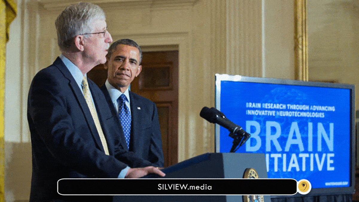
Obama, DARPA, GSK and Rockefeller’s $4.5B B.R.A.I.N. Initiative – better sit when you read
Nanotechnology Timeline
This timeline features Premodern example of nanotechnology, as well as Modern Era discoveries and milestones in the field of nanotechnology.
Premodern Examples of Nanotechnologies
Early examples of nanostructured materials were based on craftsmen’s empirical understanding and manipulation of materials. Use of high heat was one common step in their processes to produce these materials with novel properties.
 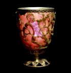 |
| The Lycurgus Cup at the British Museum, lit from the outside (left) and from the inside (right) |
4th Century: The Lycurgus Cup (Rome) is an example of dichroic glass; colloidal gold and silver in the glass allow it to look opaque green when lit from outside but translucent red when light shines through the inside. (Images at left.)
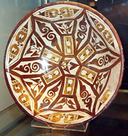 |
| Polychrome lustreware bowl, 9th C, Iraq, British Museum (©Trinitat Pradell 2008) |
9th-17th Centuries: Glowing, glittering “luster” ceramic glazes used in the Islamic world, and later in Europe, contained silver or copper or other metallic nanoparticles. (Image at right.)
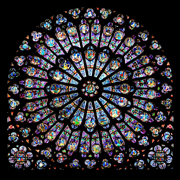 |
| The South rose window of Notre Dame Cathedral, ca 1250 |
6th-15th Centuries: Vibrant stained glass windows in European cathedrals owed their rich colors to nanoparticles of gold chloride and other metal oxides and chlorides; gold nanoparticles also acted as photocatalytic air purifiers. (Image at left.)
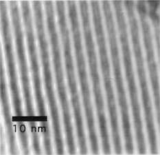
13th-18th Centuries: “Damascus” saber blades contained carbon nanotubes and cementite nanowires—an ultrahigh-carbon steel formulation that gave them strength, resilience, the ability to hold a keen edge, and a visible moiré pattern in the steel that give the blades their name. (Images below.)
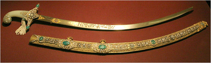 | 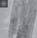 |
| (Left) A Damascus saber (photo by Tina Fineberg for The New York Times). (Right) High-resolution transmission electron microscopy image of carbon nanotubes in a genuine Damascus sabre after dissolution in hydrochloric acid, showing remnants of cementite nanowires encapsulated by carbon nanotubes (scale bar, 5 nm) (M. Reibold, P. Paufler, A. A. Levin, W. Kochmann, N. Pätzke & D. C. Meyer, Nature 444, 286, 2006). | |
Examples of Discoveries and Developments Enabling Nanotechnology in the Modern Era
These are based on increasingly sophisticated scientific understanding and instrumentation, as well as experimentation.
 |
| “Ruby” gold colloid (Gold Bulletin 2007 40,4, p. 267) |
1857: Michael Faraday discovered colloidal “ruby” gold, demonstrating that nanostructured gold under certain lighting conditions produces different-colored solutions.
1936: Erwin Müller, working at Siemens Research Laboratory, invented the field emission microscope, allowing near-atomic-resolution images of materials.
1947: John Bardeen, William Shockley, and Walter Brattain at Bell Labs discovered the semiconductor transistor and greatly expanded scientific knowledge of semiconductor interfaces, laying the foundation for electronic devices and the Information Age.
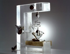 |
| 1947 transistor, Bell Labs |
1950: Victor La Mer and Robert Dinegar developed the theory and a process for growing monodisperse colloidal materials. Controlled ability to fabricate colloids enables myriad industrial uses such as specialized papers, paints, and thin films, even dialysis treatments.
1951: Erwin Müller pioneered the field ion microscope, a means to image the arrangement of atoms at the surface of a sharp metal tip; he first imaged tungsten atoms.
1956: Arthur von Hippel at MIT introduced many concepts of—and coined the term—“molecular engineering” as applied to dielectrics, ferroelectrics, and piezoelectrics
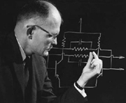 |
| Jack Kilby, about 1960. |
1958: Jack Kilby of Texas Instruments originated the concept of, designed, and built the first integrated circuit, for which he received the Nobel Prize in 2000. (Image at left.)
 |
| Richard Feynman (Caltech archives) |
1959: Richard Feynman of the California Institute of Technology gave what is considered to be the first lecture on technology and engineering at the atomic scale, “There’s Plenty of Room at the Bottom” at an American Physical Society meeting at Caltech. (Image at right.)
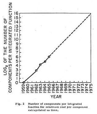 |
| Moore’s first public graph showing his vision of the semiconductor industry being able to “cram more components onto integrated circuits“ |
1965: Intel co-founder Gordon Moore described in Electronics magazine several trends he foresaw in the field of electronics. One trend now known as “Moore’s Law,” described the density of transistors on an integrated chip (IC) doubling every 12 months (later amended to every 2 years). Moore also saw chip sizes and costs shrinking with their growing functionality—with a transformational effect on the ways people live and work. That the basic trend Moore envisioned has continued for 50 years is to a large extent due to the semiconductor industry’s increasing reliance on nanotechnology as ICs and transistors have approached atomic dimensions.1974: Tokyo Science University Professor Norio Taniguchi coined the term nanotechnology to describe precision machining of materials to within atomic-scale dimensional tolerances. (See graph at left.)
1981: Gerd Binnig and Heinrich Rohrer at IBM’s Zurich lab invented the scanning tunneling microscope, allowing scientists to “see” (create direct spatial images of) individual atoms for the first time. Binnig and Rohrer won the Nobel Prize for this discovery in 1986.
1981: Russia’s Alexei Ekimov discovered nanocrystalline, semiconducting quantum dots in a glass matrix and conducted pioneering studies of their electronic and optical properties.
1985: Rice University researchers Harold Kroto, Sean O’Brien, Robert Curl, and Richard Smalley discovered the Buckminsterfullerene (C60), more commonly known as the buckyball, which is a molecule resembling a soccer ball in shape and composed entirely of carbon, as are graphite and diamond. The team was awarded the 1996 Nobel Prize in Chemistry for their roles in this discovery and that of the fullerene class of molecules more generally. (Artist’s rendering at right.)
1985: Bell Labs’s Louis Brus discovered colloidal semiconductor nanocrystals (quantum dots), for which he shared the 2008 Kavli Prize in Nanotechnology.
1986: Gerd Binnig, Calvin Quate, and Christoph Gerber invented the atomic force microscope, which has the capability to view, measure, and manipulate materials down to fractions of a nanometer in size, including measurement of various forces intrinsic to nanomaterials.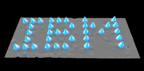
1989: Don Eigler and Erhard Schweizer at IBM’s Almaden Research Center manipulated 35 individual xenon atoms to spell out the IBM logo. This demonstration of the ability to precisely manipulate atoms ushered in the applied use of nanotechnology. (Image at left.)
1990s: Early nanotechnology companies began to operate, e.g., Nanophase Technologies in 1989, Helix Energy Solutions Group in 1990, Zyvex in 1997, Nano-Tex in 1998….
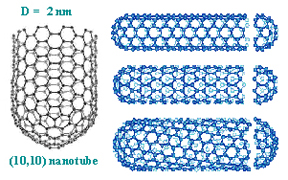
1991: Sumio Iijima of NEC is credited with discovering the carbon nanotube (CNT), although there were early observations of tubular carbon structures by others as well. Iijima shared the Kavli Prize in Nanoscience in 2008 for this advance and other advances in the field. CNTs, like buckyballs, are entirely composed of carbon, but in a tubular shape. They exhibit extraordinary properties in terms of strength, electrical and thermal conductivity, among others. (Image below.)
 | 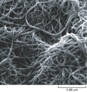 | 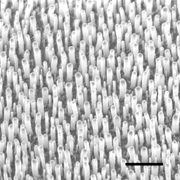 |
| Carbon nanotubes (courtesy, National Science Foundation). The properties of CNTs are being explored for applications in electronics, photonics, multifunctional fabrics, biology (e.g., as a scaffold to grow bone cells), and communications. See a 2009 Discovery Magazine article for other examples | SEM micrograph of purified nanotube “paper” in which the nanotubes are the fibers (scale bar, 0.001 mm) (courtesy, NASA). | An array of aligned carbon nanotubes, which can act like a radio antenna for detecting light at visible wave- lengths (scale bar 0.001 mm) (courtesy, K. Kempa, Boston College). |
1992: C.T. Kresge and colleagues at Mobil Oil discovered the nanostructured catalytic materials MCM-41 and MCM-48, now used heavily in refining crude oil as well as for drug delivery, water treatment, and other varied applications.
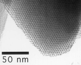 |  |
| MCM-41 is a “mesoporous molecular sieve” silica nanomaterial with a hexagonal or “honeycomb” arrangement of its straight cylindrical pores, as shown in this TEM image (courtesy of Thomas Pauly, Michigan State University). | This TEM image of MCM-41 looks at the straight cylindrical pores as they lie perpendicular to the viewing axis (courtesy of Thomas Pauly, Michigan State University). |
1993: Moungi Bawendi of MIT invented a method for controlled synthesis of nanocrystals (quantum dots), paving the way for applications ranging from computing to biology to high-efficiency photovoltaics and lighting. Within the next several years, work by other researchers such as Louis Brus and Chris Murray also contributed methods for synthesizing quantum dots.
1998: The Interagency Working Group on Nanotechnology (IWGN) was formed under the National Science and Technology Council to investigate the state of the art in nanoscale science and technology and to forecast possible future developments. The IWGN’s study and report, Nanotechnology Research Directions: Vision for the Next Decade (1999) defined the vision for and led directly to formation of the U.S. National Nanotechnology Initiative in 2000.
 |
| The progression of steps of using a scanning tunneling microscope tip to “assemble” an iron carbonyl molecule, beginning with Fe (iron) and CO (carbon monoxide) molecules (A), joining them to produce FeCO (B), then adding a second CO molecule (C), to achieve the FECO2 molecule (D). (H.J. Lee, W. Ho, Science 286, 1719 [1999].) |
1999: Cornell University researchers Wilson Ho and Hyojune Lee probed secrets of chemical bonding by assembling a molecule [iron carbonyl Fe(CO)2] from constituent components [iron (Fe) and carbon monoxide (CO)] with a scanning tunneling microscope. (Image at left.)
1999: Chad Mirkin at Northwestern University invented dip-pen nanolithography® (DPN®), leading to manufacturable, reproducible “writing” of electronic circuits as well as patterning of biomaterials for cell biology research, nanoencryption, and other applications. (Image below right.)
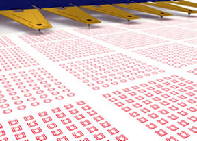 |
| Use of DPN to deposit biomaterials ©2010 Nanoink |
1999–early 2000’s: Consumer products making use of nanotechnology began appearing in the marketplace, including lightweight nanotechnology-enabled automobile bumpers that resist denting and scratching, golf balls that fly straighter, tennis rackets that are stiffer (therefore, the ball rebounds faster), baseball bats with better flex and “kick,” nano-silver antibacterial socks, clear sunscreens, wrinkle- and stain-resistant clothing, deep-penetrating therapeutic cosmetics, scratch-resistant glass coatings, faster-recharging batteries for cordless electric tools, and improved displays for televisions, cell phones, and digital cameras.
 |
2000: President Clinton launched the National Nanotechnology Initiative (NNI) to coordinate Federal R&D efforts and promote U.S. competitiveness in nanotechnology. Congress funded the NNI for the first time in FY2001. The NSET Subcommittee of the NSTC was designated as the interagency group responsible for coordinating the NNI.
2003: Congress enacted the 21st Century Nanotechnology Research and Development Act (P.L. 108-153). The act provided a statutory foundation for the NNI, established programs, assigned agency responsibilities, authorized funding levels, and promoted research to address key issues.
 |
| Computer simulation of growth of gold nanoshell with silica core and over-layer of gold (courtesy N. Halas, Genome News Network, 2003) |
2003: Naomi Halas, Jennifer West, Rebekah Drezek, and Renata Pasqualin at Rice University developed gold nanoshells, which when “tuned” in size to absorb near-infrared light, serve as a platform for the integrated discovery, diagnosis, and treatment of breast cancer without invasive biopsies, surgery, or systemically destructive radiation or chemotherapy.2004: The European Commission adopted the Communication “Towards a European Strategy for Nanotechnology,” COM(2004) 338, which proposed institutionalizing European nanoscience and nanotechnology R&D efforts within an integrated and responsible strategy, and which spurred European action plans and ongoing funding for nanotechnology R&D. (Image at left.)
2004: Britain’s Royal Society and the Royal Academy of Engineering published Nanoscience and Nanotechnologies: Opportunities and Uncertainties advocating the need to address potential health, environmental, social, ethical, and regulatory issues associated with nanotechnology.
2004: SUNY Albany launched the first college-level education program in nanotechnology in the United States, the College of Nanoscale Science and Engineering.
2005: Erik Winfree and Paul Rothemund from the California Institute of Technology developed theories for DNA-based computation and “algorithmic self-assembly” in which computations are embedded in the process of nanocrystal growth.
 |
| Nanocar with turning buckyball wheels (credit: RSC, 29 March 2006). |
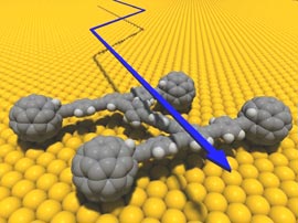
2006: James Tour and colleagues at Rice University built a nanoscale car made of oligo(phenylene ethynylene) with alkynyl axles and four spherical C60 fullerene (buckyball) wheels. In response to increases in temperature, the nanocar moved about on a gold surface as a result of the buckyball wheels turning, as in a conventional car. At temperatures above 300°C it moved around too fast for the chemists to keep track of it! (Image at left.)
2007: Angela Belcher and colleagues at MIT built a lithium-ion battery with a common type of virus that is nonharmful to humans, using a low-cost and environmentally benign process. The batteries have the same energy capacity and power performance as state-of-the-art rechargeable batteries being considered to power plug-in hybrid cars, and they could also be used to power personal electronic devices. (Image at right.)
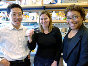 |
| (L to R) MIT professors Yet-Ming Chiang, Angela Belcher, and Paula Hammond display a virus-loaded film that can serve as the anode of a battery. (Photo: Donna Coveney, MIT News.) |
2008: The first official NNI Strategy for Nanotechnology-Related Environmental, Health, and Safety (EHS) Research was published, based on a two-year process of NNI-sponsored investigations and public dialogs. This strategy document was updated in 2011, following a series of workshops and public review.
2009–2010: Nadrian Seeman and colleagues at New York University created several DNA-like robotic nanoscale assembly devices. One is a process for creating 3D DNA structures using synthetic sequences of DNA crystals that can be programmed to self-assemble using “sticky ends” and placement in a set order and orientation. Nanoelectronics could benefit: the flexibility and density that 3D nanoscale components allow could enable assembly of parts that are smaller, more complex, and more closely spaced. Another Seeman creation (with colleagues at China’s Nanjing University) is a “DNA assembly line.” For this work, Seeman shared the Kavli Prize in Nanoscience in 2010.
2010: IBM used a silicon tip measuring only a few nanometers at its apex (similar to the tips used in atomic force microscopes) to chisel away material from a substrate to create a complete nanoscale 3D relief map of the world one-one-thousandth the size of a grain of salt—in 2 minutes and 23 seconds. This activity demonstrated a powerful patterning methodology for generating nanoscale patterns and structures as small as 15 nanometers at greatly reduced cost and complexity, opening up new prospects for fields such as electronics, optoelectronics, and medicine. (Image below.)
 |
| A rendered image of a nanoscale silicon tip chiseling out the smallest relief map of the world from a substrate of organic molecular glass. Shown middle foreground is the Mediterranean Sea and Europe. (Image courtesy of Advanced Materials.) |
2011: The NSET Subcommittee updated both the NNI Strategic Plan and the NNI Environmental, Health, and Safety Research Strategy, drawing on extensive input from public workshops and online dialog with stakeholders from Government, academia, NGOs, and the public, and others.
2012: The NNI launched two more Nanotechnology Signature Initiatives (NSIs)–Nanosensors and the Nanotechnology Knowledge Infrastructure (NKI)–bringing the total to five NSIs.
2013:
-The NNI starts the next round of Strategic Planning, starting with the Stakeholder Workshop.
-Stanford researchers develop the first carbon nanotube computer.
2014:
-The NNI releases the updated 2014 Strategic Plan.
–The NNI releases the 2014 Progress Review on the Coordinated Implementation of the NNI 2011 Environmental, Health, and Safety Research Strategy.
To be continued?
Our work and existence, as media and people, is funded solely by our most generous supporters. But we’re not really covering our costs so far, and we’re in dire needs to upgrade our equipment, especially for video production.
Help SILVIEW.media survive and grow, please donate here, anything helps. Thank you!
! Articles can always be subject of later editing as a way of perfecting them

You can even eat some of them.
CLICK HERE
